I got an HP Envy laptop in 2017, and though this laptop got me through much of high school and college, it’s been slowing down a lot in recent years. Since the screen was broken, and donation programs in MA won’t take laptops with broken glass, I decided to do a teardown and look inside.
Generally, I was impressed with the mechanical construction and electrical design - there were a lot of screws, yes, but they were all the same size (making disassembly easy). Obviously, this is a large company that invests a lot of resources into making quality laptops.
Something I was surprised by was the lack of ferrite beads, which are generally added to reduce emissions radiating from a cable in order to pass FCC compliance. I can think of a few reasons why - the laptop is pretty compact so there aren’t enough cables to create antennas, and the entire outside is metal so it acts as a Faraday cage, attenuating quite a bit of radiation.
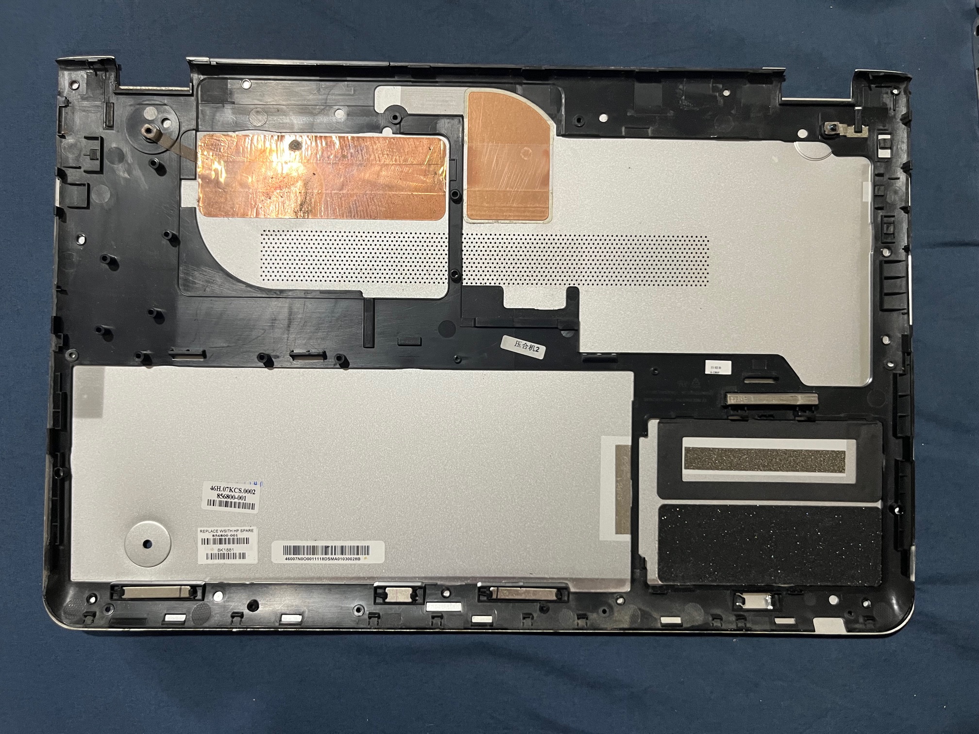
I started by taking off the back cover, revealing the electronics inside.
The back isn’t terribly interesting - it mostly has mechanical features and an air intake.
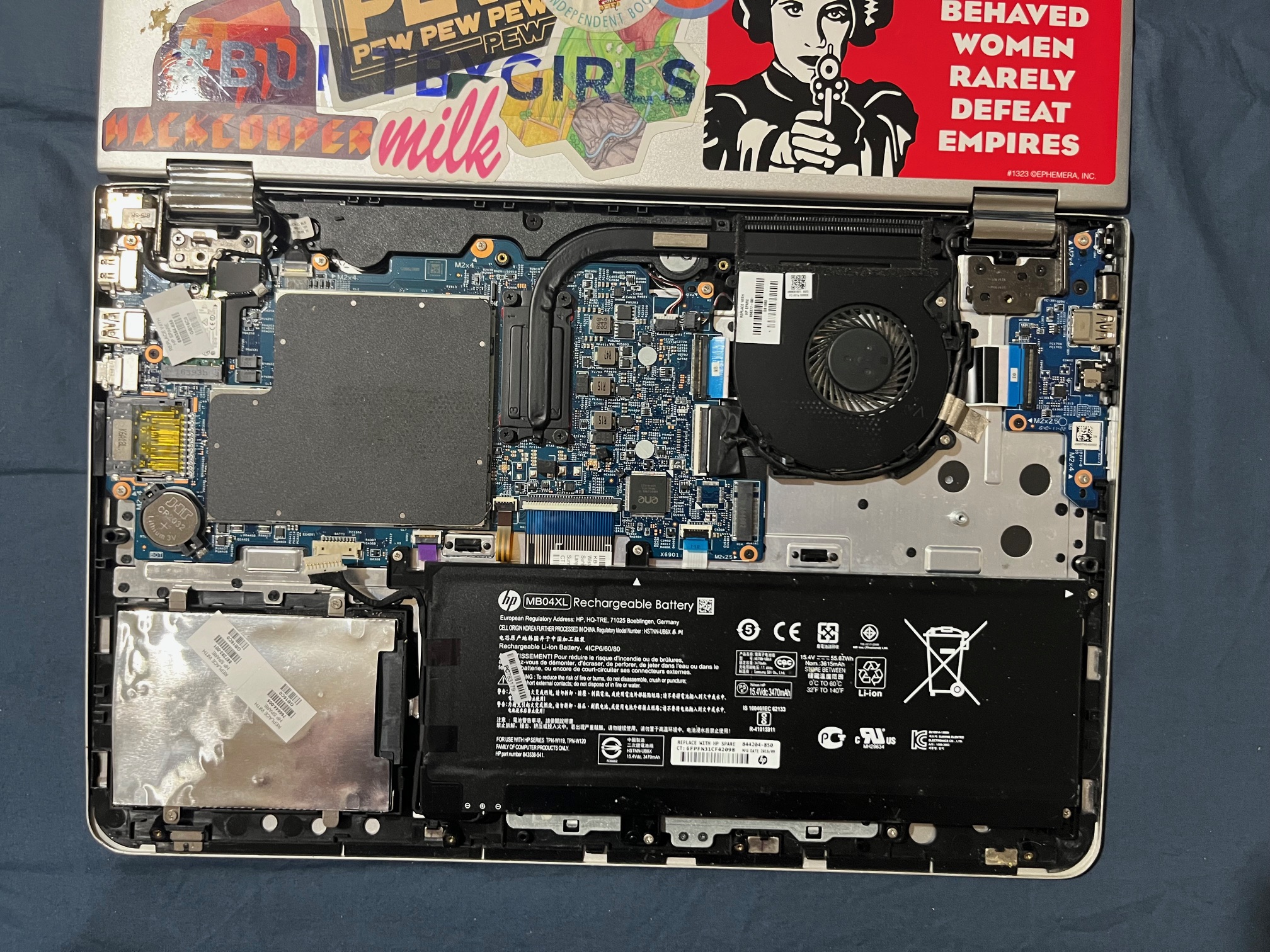
I started by removing the battery. Safety first!
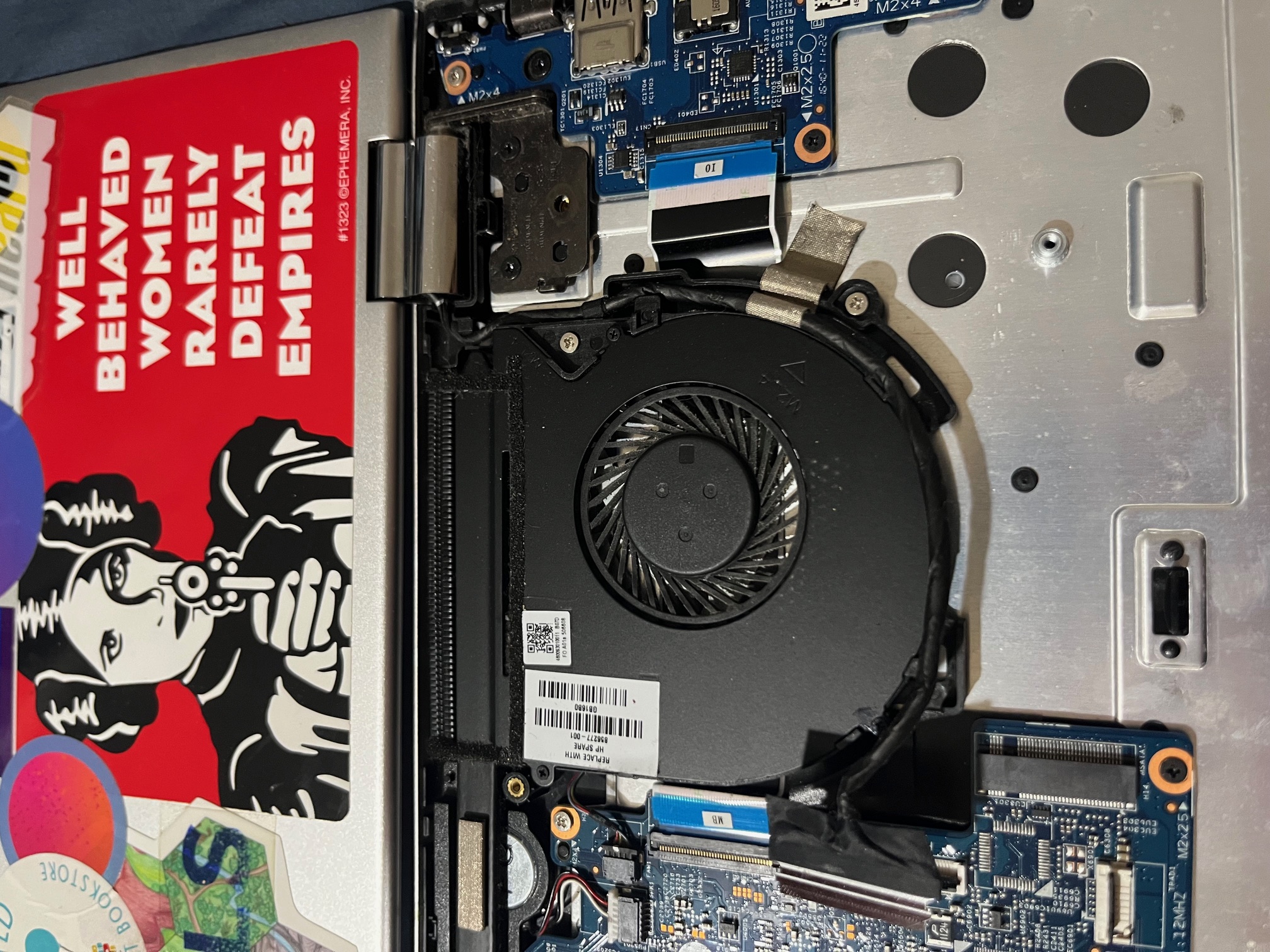
I noticed some conductive tape from the touchpad board to the metal chassis, which makes sense - I’d think any component being touched by users is most susceptible to static discharge. Adding tape like this is probably the easiest way to address ESD since you wouldn’t want any screws in a touchpad that could feel weird to the user or interfere with clicking motions.
Same for the fan cable - a plastic housing would need a connection to ground to avoid charges building up, especially since the fan is so close to a flex cable that handles USB signals.
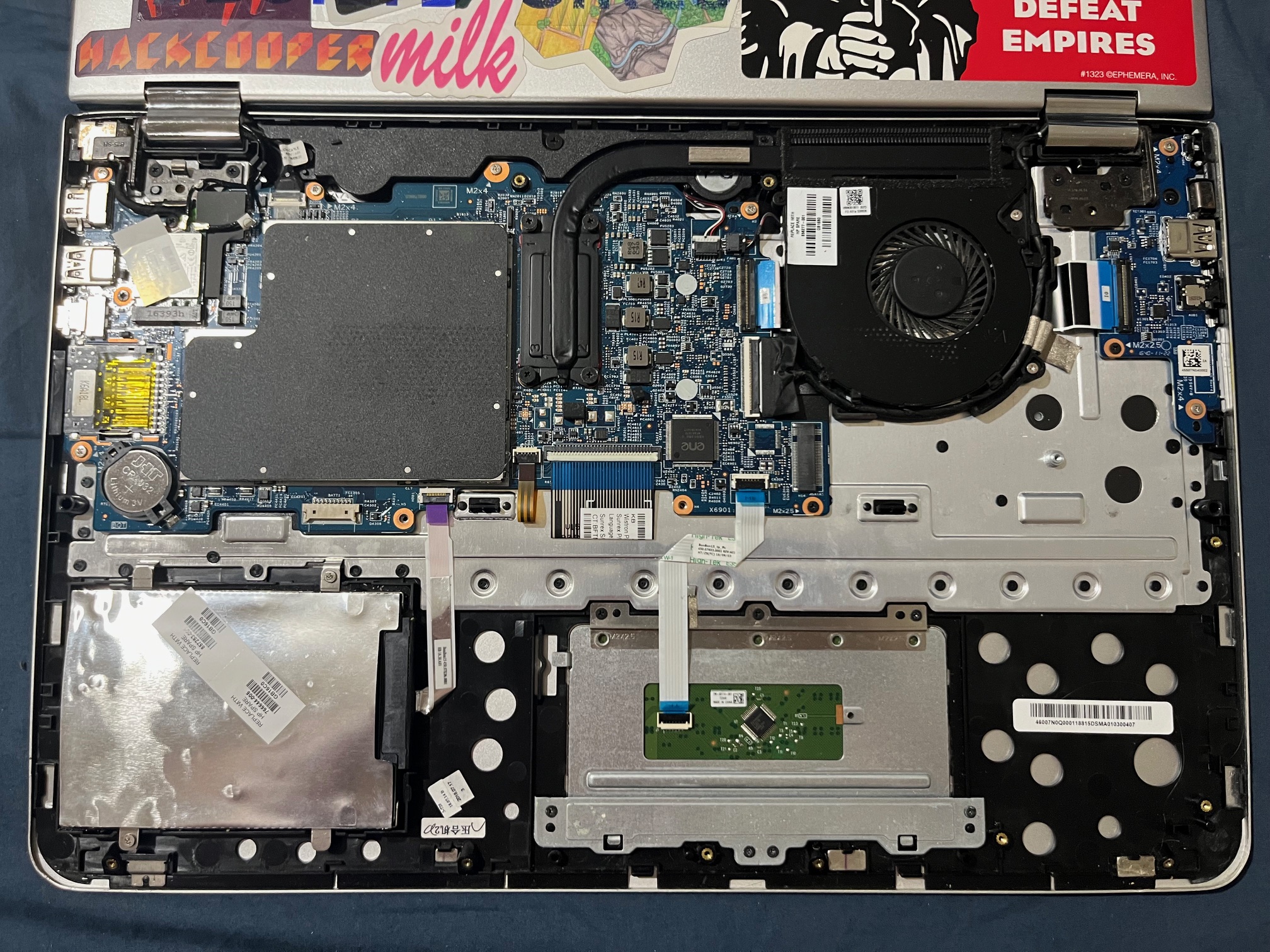
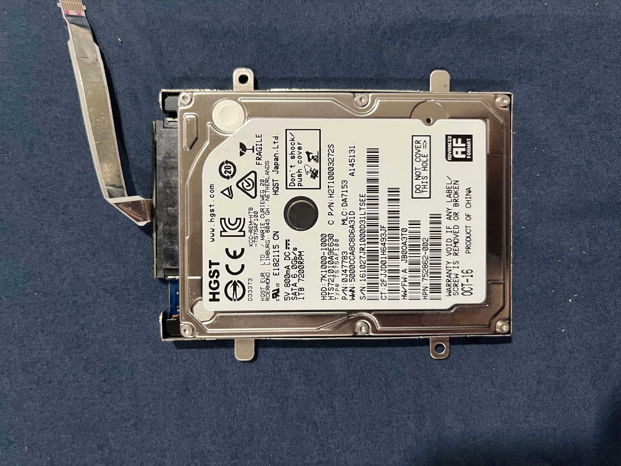
I took out the hard drive, a 1TB SATA III drive - which is still pretty capable in today’s PC landscape. Although I backed up the hard drive and wiped it before taking this apart, I’ll probably keep this one around since it’s still pretty performant, although it’s not the more modern SSD technology.
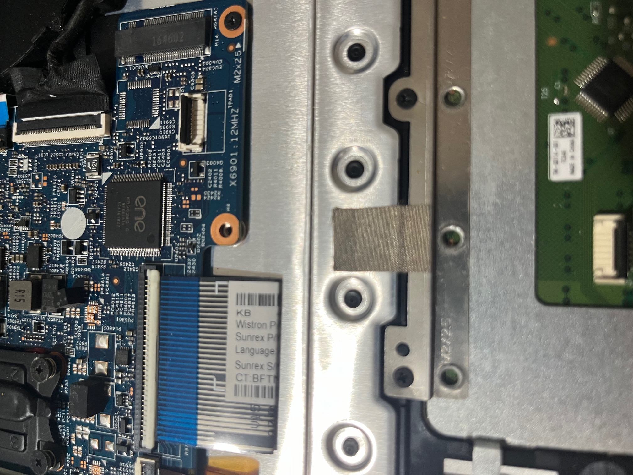
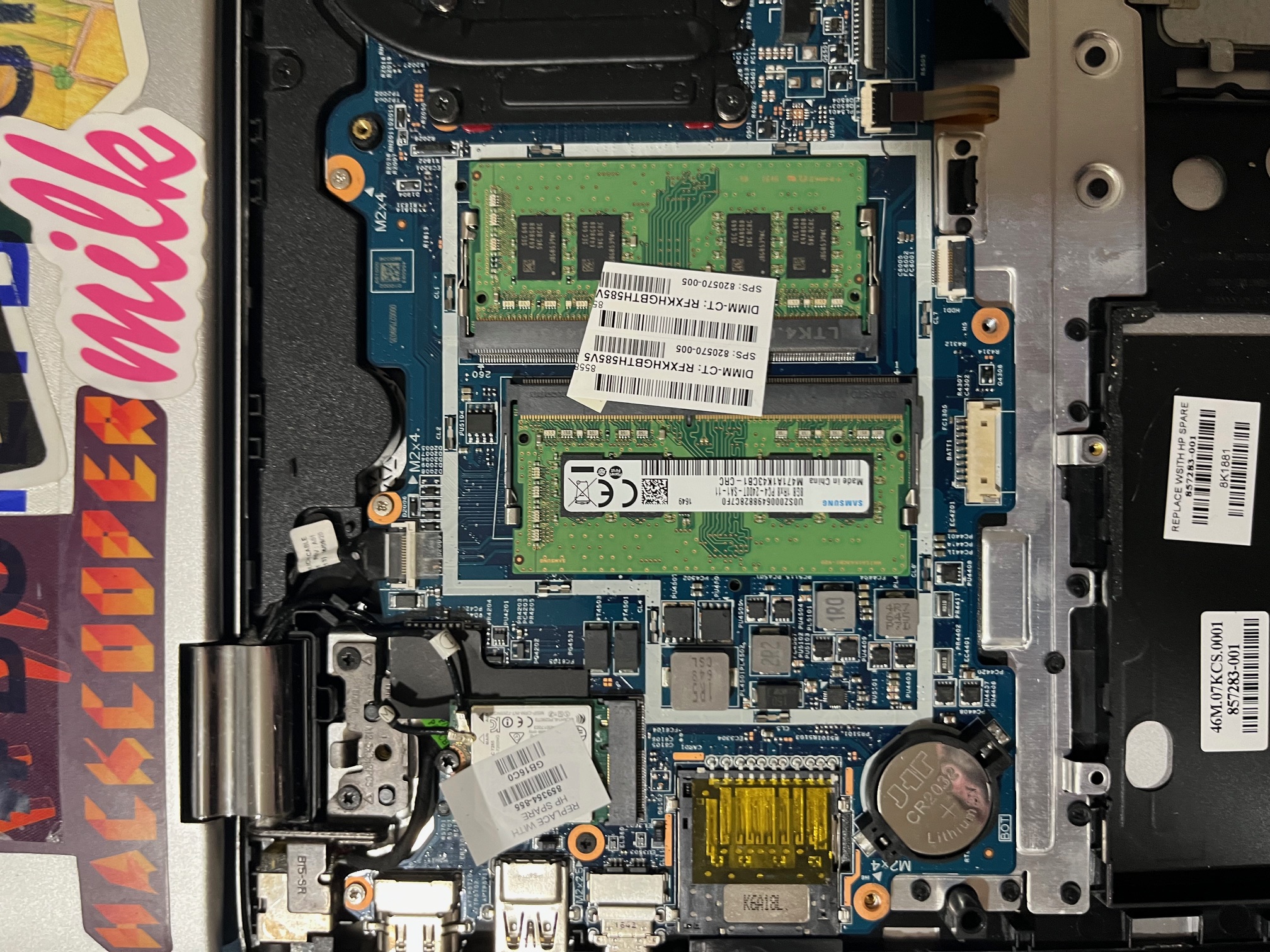
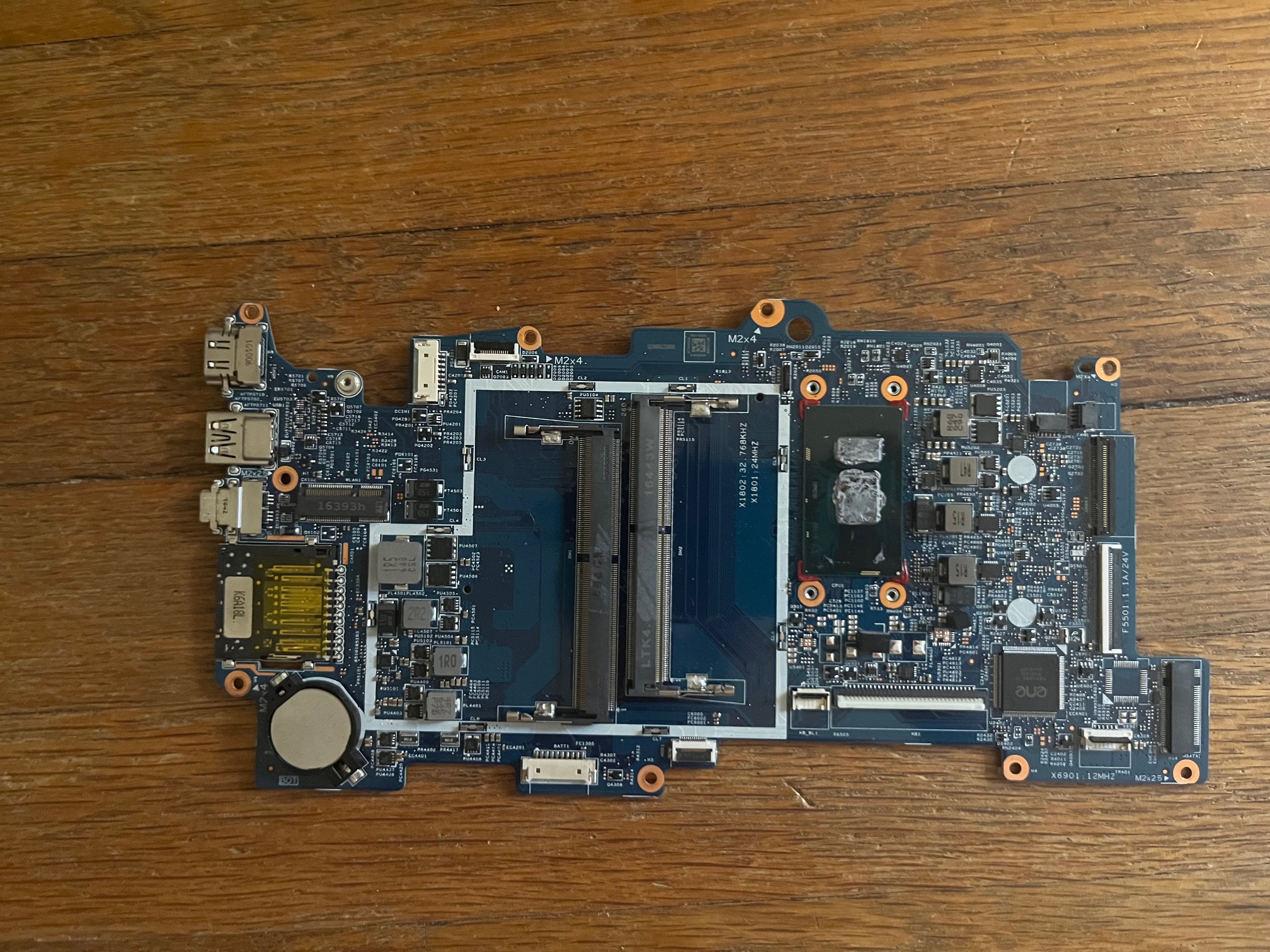
Next, onto the motherboard. There’s an RF shield over some of the more sensitive components, most notably the RAM. Really important to protect that from interference, and it has the added benefit of preventing radiation from the RAM as well.
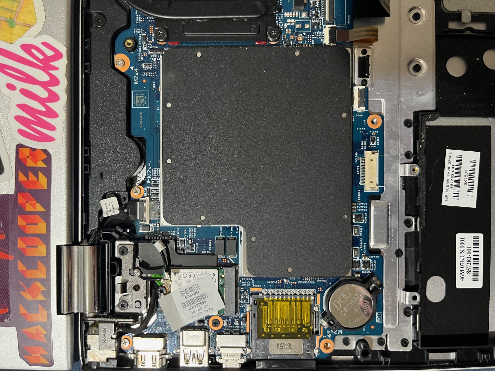
I found it interesting that there were two main PCBs, connected by a flex cable. I imagine this was for packaging reasons. Plus, the higher speed interfaces (HDMI) were on the main board, closer to the processing, while the slower interfaces (USB2, power button) that are more forgiving of errors were on the smaller board.
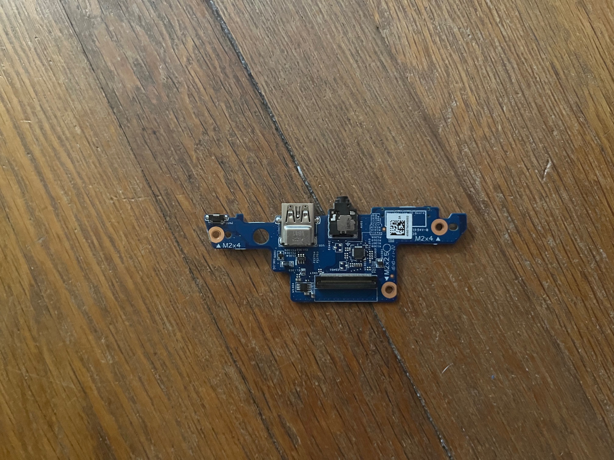
Quick sidebar - I always think it’s interesting how even high-end electronics use cheap-looking connectors on the inside, and that’s because they work just fine! This is true for the connectors here and especially the power button - not sure what I expected under the nicely industrial-designed oval button on the laptop case, but it was a silly little button (which has seen lots of use over the past seven years so I’m not surprised it’s not as resilient as it used to be).
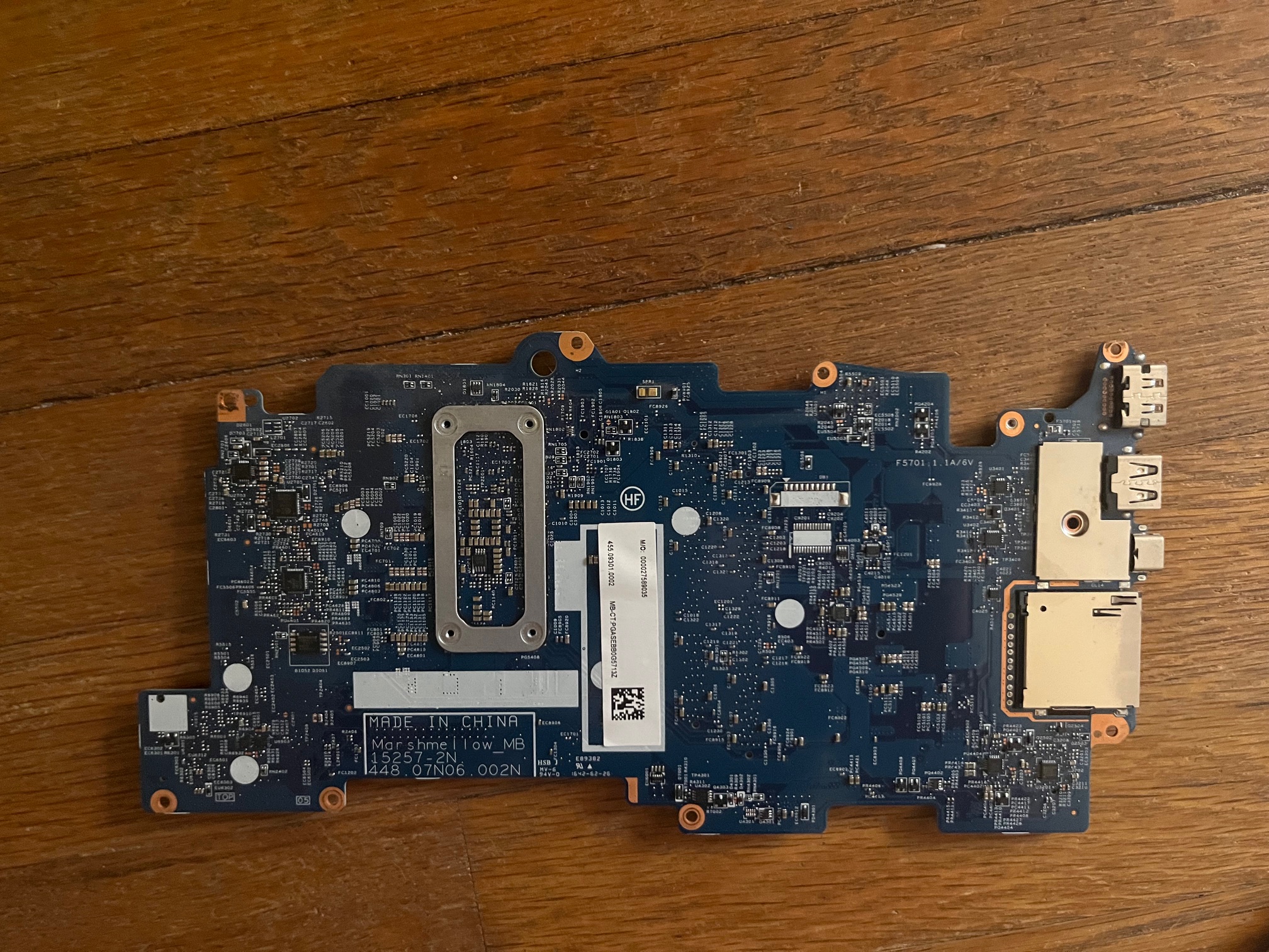
Here’s the motherboard! I noticed the motherboard was named “Marshmallow,” which must have been the code name for this project, which I find really cute :) I also noticed they labeled every single passive, even the tiny ones, which is impressive on a board of this size. This is some really dense placement.
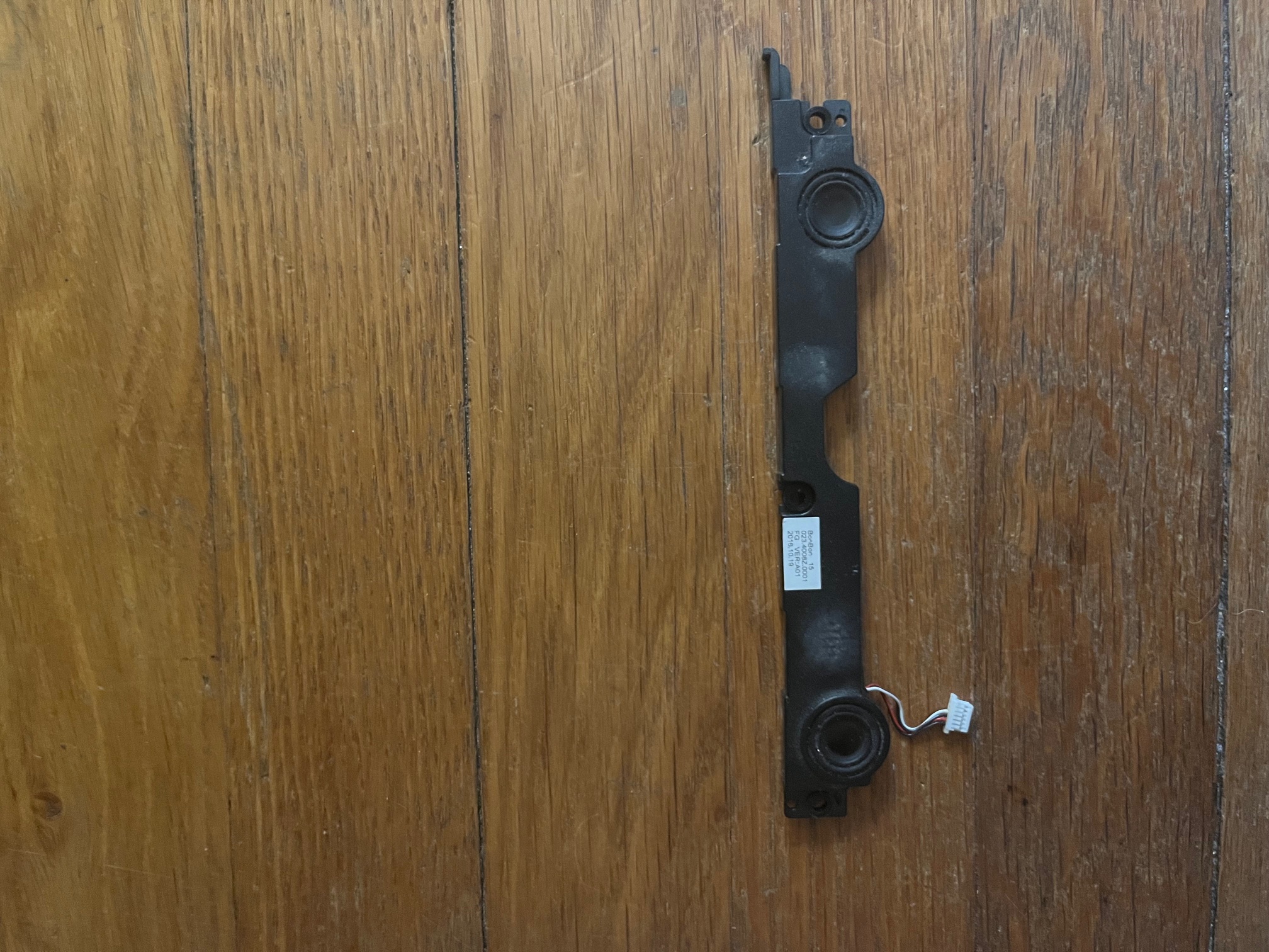
I was also impressed by how small the speakers were for their sound - those things got pretty loud! I also think it’s interesting how you can see the dust pattern from years of use (initially pop punk in high school, although my music taste has diversified since then).
I didn’t really want to touch the screen (broken glass and all that), but I found that once I disconnected it from the bottom of the laptop, the hinges got a lot harder to move. The Envy can turn into a tablet, so its hinges have a 180 degree range of motion. Packaging a high-speed cable to interface with an LCD when nothing is moving is really hard (I’d know, having worked on this for the Form 4). I can’t even imagine having to maintain good signal quality over repetitive movements. I must have disturbed that careful balance they struck by moving the cable. In all my years of owning this laptop, I’ve never had an issue with the display or with the hinging mechanicsm. This must have been a really tough thing to accomplish for a team of electrical, mechanical, and optical engineers - so many congrats to them!
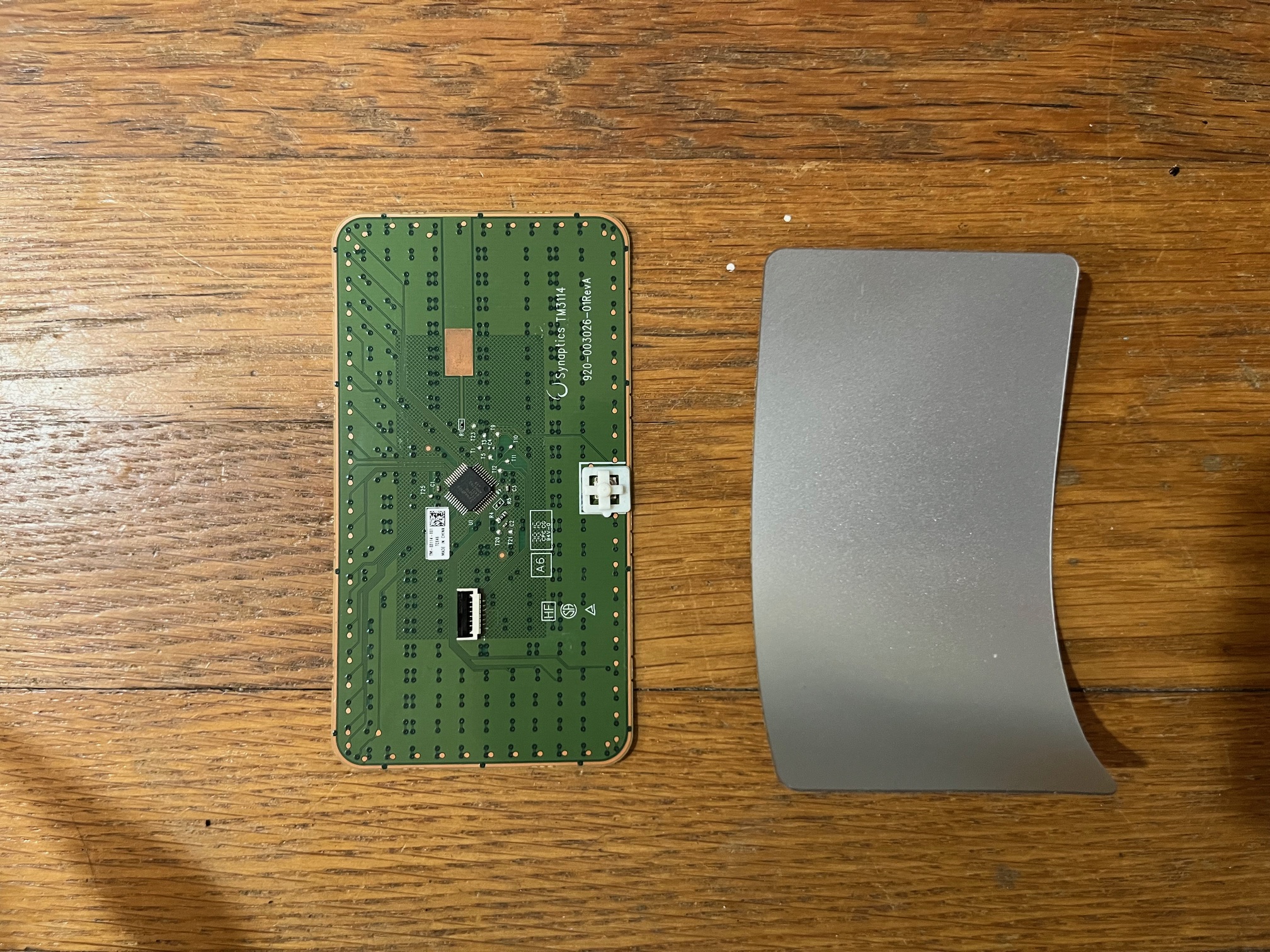
Finally, I took the touchpad out and found that it was essentially a capacitive touch sensing PCB from Synaptics - it doesn’t seem to have been designed by HP. The spacing of the sensors doesn’t seem even in the y axis, so I’m curious how that was determined.
This laptop has been there for me during so many important moments - from writing college essays to signing my new grad job offer. It feels full circle that I understand so much more about its inner workings and the choices that went into making it now than I could have when I first got it.
Comments